Thermal transport mapping in twisted double bilayer graphene
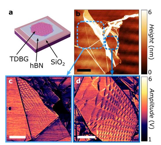
Two-dimensional (2D) materials have attracted significant interest due to their tunable physical properties when stacked into homo- and heterostructures. Twisting adjacent layers introduces moiré patterns that strongly influence the material’s electronic and thermal behavior. In twisted graphene systems, the twist angle critically alters phonon transport, leading to reduced thermal conductivity compared to Bernal-stacked configurations. However, experimental investigations into thermal transport in twisted structures remain limited. Here, we study the local thermal properties of low-angle ( ) twisted double bilayer graphene using scanning thermal microscopy. We find an increase in thermal resistance of KW−1 compared to untwisted bilayers, attributed to changes in both intrinsic thermal conductivity and the tip–sample interface. Analytical modeling shows that such variations may be attributed to intrinsic conductivity changes or modifications of the tip–sample interface resistance, or a combination of both. Our study highlights how twist alters the overall thermal resistance network in graphene heterostructures, providing direct nanoscale evidence that moiré engineering impacts multiple pathways of heat dissipation. These insights advance understanding of thermal transport in twisted 2D systems and open avenues for thermal management in twistronic devices.
Thermal transport mapping in twisted double bilayer graphene Read More »